
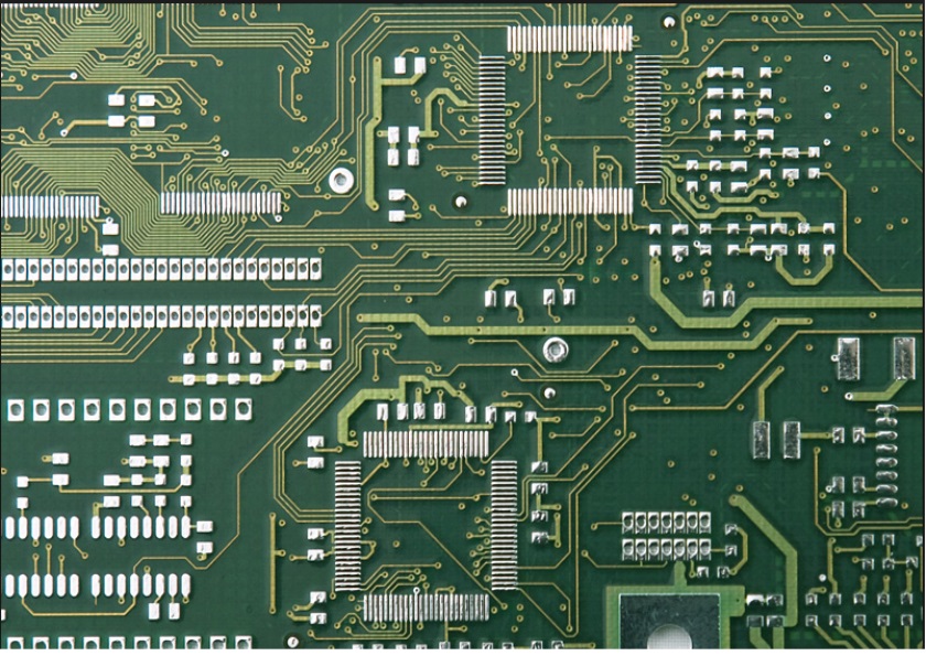
The Magic Behind Multilayer PCB Design
Ever wondered how multilayer PCBs work their magic? Brace yourself, because we’re about to unveil the secrets behind their extraordinary performance.
In this article, you’ll discover the advantages of multilayer PCBs, explore key design considerations, and learn how to overcome the challenges that come with their intricate design.
Get ready to become a master of creating high-performance multilayer PCBs as we guide you through the fascinating world where technology and craftsmanship intertwine.
So, let’s dive in and unravel the enchanting realm of multilayer PCB design.
Advantages of Multilayer PCBs
Multilayer PCBs offer numerous advantages, making them a preferred choice for electronic design engineers.
One of the key benefits of multilayer PCBs is their efficient manufacturing process. Unlike single-layer or double-layer PCBs, which require additional wiring and components, multilayer PCBs integrate multiple layers into a single board. This streamlines the manufacturing process, reducing the time and effort required for assembly.
Additionally, multilayer PCBs are highly cost-effective. By consolidating multiple layers onto a single board, engineers can reduce the overall size and weight of the electronic device, resulting in lower production costs.
Moreover, the compact design of multilayer PCBs allows for increased functionality in smaller devices, making them ideal for portable electronic gadgets.
Key Design Considerations
When considering the design of multilayer PCBs, it’s important to take into account key factors that will impact the overall functionality and performance of the electronic device.
To ensure signal integrity optimization and efficient operation, there are specific stackup design considerations that need to be addressed:
– **Layer arrangement**: Determine the number of layers required based on the complexity of the circuit and the density of components.
– **Power and ground planes**: Include dedicated power and ground planes to minimize noise and provide stable voltage references.
– *Plane distribution*: Distribute power and ground planes evenly throughout the PCB to maintain uniform impedance.
– *Plane separation*: Separate power and ground planes to reduce crosstalk and electromagnetic interference.
Overcoming Challenges in Multilayer PCB Design
To overcome challenges in designing multilayer PCBs, you can start by carefully selecting the appropriate materials and technologies. One common mistake is choosing the wrong substrate material, which can lead to signal integrity issues and poor performance. By understanding the requirements of your design and selecting the right substrate material, such as FR-4 or high-frequency materials like PTFE, you can ensure the desired electrical performance.
Another challenge is managing heat dissipation in densely packed multilayer PCBs. Thermal vias, heat sinks, and proper component placement can help dissipate heat effectively.
Troubleshooting techniques, such as using impedance measurement tools and signal integrity analysis, can help identify and resolve issues related to signal integrity and power integrity.
Tips for Creating High-Performance Multilayer PCBs
Start by optimizing your component placement and routing for efficient signal flow. This is crucial for creating high-performance multilayer PCBs. Here are some tips to help you achieve this:
Material selection:
– Choose high-quality and reliable materials for your PCBs. Consider factors such as dielectric constant, thermal conductivity, and mechanical strength.
– Select materials with low loss tangent and low dispersion to minimize signal degradation and maintain signal integrity.
Signal integrity optimization:
– Use proper ground and power planes to reduce noise and maintain signal integrity.
– Minimize the length and number of vias to reduce signal reflections and losses.
– Follow best practices for trace routing, such as avoiding sharp angles and crossing traces.
Conclusion
Congratulations! You have now unlocked the magic behind multilayer PCB manufacturers design. By harnessing the power of multiple layers, you can create high-performance PCBs that are more compact, efficient, and reliable.
Remember to carefully consider key design considerations and overcome challenges to achieve optimal results.
With these tips and your newfound knowledge, you can bring your electronic creations to life with precision and finesse.
So, dive into the world of multilayer PCB design and let your imagination soar!